Greetings! Most of my future homebrew radio projects will focus on building radio astronomy gear.

Radio astronomy offers much fun + learning for the radio homebuilder -- example topics include how to design and make antennas, LNAs, receivers, and frequency synthesizers from HF to microwave. Further we may craft op-amp analog integrators to remove background noise, and/or ADCs, plus write software to store and analyze our data. Avid radio astronomers enjoy a strong understanding of noise measurement/physics, plus a whole lot of really cool science. I've already made new friends and feel inspired by the dedicated, skillful folks who listen to signals from space on stuff they craft in their home labs. In radio astronomy, Dx might mean receiving signals from 590 million kilometers away. I'm in!
Listening to the Jovian bursts from Jupiter seems a good place to start. Single sideband radio telescope receivers from about 18 - 24 MHz work for Jupiter, however, the single most common frequency = 20.1 MHz. Listening at 20.1 MHz avoids 20 MHz WWV and lies above the earth's ionospheric cut-off frequency avoiding some human caused night-time interference.
For my Jupiter receiver, I sought a 20.1 MHz or so local oscillator with a little frequency agility to steer around local interference. Invigorated by 4 months of studying PLL design, for Radionova 1, I built a simple, from-scratch PLL-based synthesizer that runs from ~20.117 to 20.666 MHz with no MCU.
With sincere thanks, I borrow heavily from the published work of Wes, W7ZOI.

I suggest you study published PLL books plus read the many great online articles concerning PLL-based synthesizers, demodulators and quadratures since I'm a mere beginner when it comes to PLL knowledge and experience.
Reference Oscillator

Above — Reference oscillator schematic. A low noise 2 MHz signal gets digitized by a BJT switch offering the correct voltage swing to properly clock an intriguing CMOS level circuit I learned about from Wes. The 74HC193 and 74HC74 4-bit ripple counter + D flip flop perform the division where R = 3 to 17. Each R gets chosen by flipping 4 front-panel mounted toggle switches.
Wes once shared that the divider scheme idea essentially came from the 74HC193 data sheet where they show what happens when its plied as a down counter ( where you load a number and then count down until it reaches 0 ). That number gets augmented by 2. 1 comes from the HC7474 D-FF that follows the 74HC193, while the other comes from the phasing of the signals. The HC7474 makes the overall output coherent with the clock and eliminates the flicker noise that might be generated by the longer divider chain inside the 74HC193.
In this PLL synthesizer, the VCO does not get divided, so N = 1 — thus it avoids the usual 20 log N phase noise addition when the reference frequency is multiplied up to get the VCO frequency.


Above — 'Scope capture of the reference oscillator transistor switch output now at CMOS drive level to clock the reference oscillator divider circuitry.

Above — Table of all possible switch settings, the division integer R, the resultant VCO frequency and
the varactor tuning DC voltage as measured on the output of the VCO filter on the PLL board. That's the DC voltage that changes the VCO frequency within the loop. To lower noise, it's important to keep a couple of volts DC or so on the VCO varactors at your lowest frequency. Further, I noticed if the varactor tuning voltage drops below ~ 0.4 VDC, the loop may suffer instability.


Above — Reference oscillator breadboard prototype
Offset Mixer

Above — Offset mixer schematic. The 20.XXX MHz signal from the VCO offset mixer port gets attenuated 6 dB to establish the correct drive needed to eliminate excessive distortion in the mixer output. The maximum input signal power into the 50 Ω input port = -4 dBm from my experiments.
The mixer output [ 20.XXX MHz signal - 20 MHz crystal frequency ] gets low-pass filtered and then digitized to drive 1 of the the D-FFs in the PFD. In the Jupiter receiver, exact frequencies rank unimportant, so I didn't correct the 20 MHz crystal-based oscillator frequency exactly to 20.0 MHz with a trimmer as shown in the inset.

Above — The low-pass filtered offset mixer output measured with a 10X 'scope probe. A simple low-pass filter seems so trivial compared to the usual triple tuned band-pass filters we must design and employ following mixers in circuitry like transmit mixer chains. Love this. You'll see simple, pi low-pass filters after offset mixers in old CB radio synthesizers and also in some of Wes' work.
I studied the PLL circuitry of countless radios + signal generators and continue my reading today.

Above — 'Scope capture taken on the collector of the BJT switch — ready to drive the CMOS level logic of the PFD.

Above — Offset mixer breadboard. I used tons of caps as standoffs for my DC lines.
VCO

Above — VCO schematic. I spent 4 months studying how to design PLL circuitry and so the buffers on this particular VCO look a little crazy. Since we have 3 oscillators running at low frequency to high frequency, signals can travel along DC power lines, connecting signal cables and possibly through capacitive coupling. This VCO buffer was designed to eliminate signal flow down wires to allow careful examination of PLL loop filtration without contamination due to the aforementioned issues.
I normally don't make such extravagant buffers for my VCOs.
A ripple filter helps eliminate any noise riding on the DC supply to a very standard JFET Colpitts oscillator. I determined the VCO capacitor and inductor values by scaling the X (reactance) values in ohms from the Colpitts VCO caps and inductor from EMRFD Figure 4.34.
If you view the synthesizers in professional radios, you'll nearly always see a ripple filter on the DC going to VCO stages. The reason might not be obvious — the greatest source of spurious amplitude modulation within a PLL = the DC supply. Unwanted signals bumping along the DC line or their harmonics may enter RF stages and get amplitude modulated. We ought to well filter our DC lines! Not-to-mention PLLs are very prone to phase modulation and again a low ripple power supply helps the cause. Applying low noise voltage regulators may also help. In my VCO, I simply avoided a voltage regulator and my main DC power supply is well filtered.
Further, to minimize phase modulation, I chose a low gain VCO. In the math, that's the KVCO value expessed in Hz/v or KHz/volt -- or even rad/s/v. A good way to envision KVCO = the effect the op-amp controller output has on the VCO frequency (including the VCO to op-amp interface components). Ideally, the VCO should vary as linearly as possible with controller output voltage changes and the full controller output voltage range should map to the full VCO frequency range.
I designed the buffers to feature very light coupling and just enough current to not add harmonic distortion to the signal as the passes through the source followers to each low impedance output port.

Above — A 'scope or DSO capture of my 2 output signals from the VCO with frequency control provided by a temporary 10K 'tuning' potentiometer hooked to the 12.3 VDC supply. To ensure proper function and ease troubleshooting, it's good to test your VCO before hooking it up to PLL circuitry. The yellow channel goes to the offset mixer, while the blue channel is the main VCO output.

Above — A spectrum analyzer capture of the VCO set to 20.1 MHz taken at the port that goes to the offset mixer. The second harmonic lies at 34.5 dBc. The instrument's clock made 1 of the spikes at 10 MHz.

PLL
I'll show some some PLL board details, but won't go into the math required to properly design a main loop filter since numerous books and websites cover this material in great depth.

Above — The final PLL circuitry from Radionova 1.
We live in a time of 1 chip frequency synthesizers. With a
microcontroller, some input/output hardware and several lines of code, we can
make easy synthesizers at low cost. If
our project's digital noise and particular close-in phase noise requirements
get demanding (especially as we move up in frequency), it takes a little more
finesse and thought to implement our frequency synthesizer.
Homebrewing with discrete components seems
like yesterday’s answer, however, for builders with limited computer
programming skills [ actually, many builders just copy others people’s code ]
and/or for those who want to learn about PLLs in depth – discrete homebrew synthesizers
provide 1 option to learn the ropes.
PLL Discussion
The PLL is a negative feedback, or servo system designed to keep
a minimum phase error between the VCO signal and a Reference signal which in simple synthesizers
get divided down as N and R divider chains respectively. The phase error gets compared in a phase detector or phase frequency detector [ PFD ] The PFD offers the advantage that it will try to synchronize the VCO to
both the frequency and phase of the reference signal.
Once the phase error reaches its minimum, at somewhere near to 0 degrees, we term the PLL as locked.
I employed the popular PFD which
uses 2 edge-triggered D flip-flops with their D inputs tied to logic HIGH plus a NAND gate in the reset path that resets the flip-flops when both FF outputs go high simultaneously.
The PFD produces a pulsating signal proportional to the phase difference
between the incoming signals. You can watch these pulses in your 'scope.
Serving
as an integrator plus a low-pass filter, the
loop filter sets the dynamic characteristics of the PLL and drives the VCO
varactors with a DC voltage that goes up and down as needed to minimize the
phase error in the PFD.
A problem exists with PFDs called the dead zone. When in phase lock with the phase error near
0, a situation exists where the output control
voltage isn't a function of the phase difference between the reference and the
VCO signals. Caused intrinsically by logic
delay times plus the D-FF reset time, dead zone error potentially leads to reference spurs in the
VCO output, plus feedback loop jitter and thus
phase noise. The dead zone problem worsens with lower reference frequencies.


Above — Another solution to the dead zone problem --- place an offset to keep the flip-flops from simultaneously switching together.
The 100K or so resistor injects a current that causes a phase offset. The loop must then operate at a phase other than 0 degrees for it to be closed and solves the problem of simultaneous FF switching.
Both the reset gate delay and offset methods shown above may introduce phase noise into the VCO. You'll find some papers on this topic with your favorite search engine.
Loop Filtration
PLL filters remove unwanted high frequency components and noise that appears on the VCO tuning line and ultimately as noise on the VCO output signal by means such as phase modulation.
A basic op-amp loop filter may lack effective filtration of the high frequency noise exiting the PFD, so 2 additional filters may be added: a phase detector filter and a VCO filter.
Many books cover loop filter design and you may simplify this process with software or a spreadsheet to perform the calculations. I won’t cover loop filter design except to discuss it in the context of designing the phase and VCO filters shown on my PLL board schematics above.
To design a proper main loop filter, you must carefully consider aspects such as a the N, damping ratio, VCO characteristics -- and the closed loop bandwidth. Often enough, we'll chose a closed loop bandwidth no higher than ~ 1/10th of the minimum input frequency, however, other practical factors loom such as the 1/F noise corner frequency of the op-amp or active device(s) used in the VCO. Please refer to PLL design textbooks and article for details.
We might choose the phase and VCO filters cut-off values based upon our main loop filter's closed loop bandwidth -- and a time-tested starting value for both is to design a low-pass cutoff frequency of 10 times the closed-loop bandwidth. A delicate dance ensues: too low a cutoff frequency and your loop oscillates -- too high a cutoff and these added filters may work poorly.
The phase filter smooths out fast edges from the PFD logic to rates that can handled by op-amp. The phase filter also helps to attenuate input signal + harmonics to minimize VCO modulation. Again chose a as low a cutoff frequency as possible -- but not too low to trigger loop instability and oscillations. As aforementioned: perhaps start with a phase filter cutoff frequency of 10 times the closed loop bandwidth.
The VCO filter also attenuates PFD signals to minimize VCO modulation and jitter. Like the phase filter, a recommended starting cutoff frequency is 10 times the closed loop bandwidth of your main loop filter.

Above — The frequency response of my entire PLL filter system

Above — Spectrum analyzer screen capture of my VCO signal at 20.116 MHz with a 500 KHz span. I can't see my reference sidebands which is good, but the poor phase noise and filter skirt shape of my spectrum analyzer make it impossible to know whats going on in terms of close-in phase noise. That's another measurement story.
I adjusted the RC values in my phase and VCO filters to intentionally destabilize the loop and see what happens. What hath I wrought? See below:

Above — I placed 10X scope probes on the offset mixer output, the output of my phase frequency detector and also watched the output in frequency domain on a spectrum analyzer. Things get rather ugly when you throw a negative feedback PLL into oscillation.
Tests
I posit that a PLL might be the most interesting circuit you can study on your bench. With a 10X 'scope probe on the output of the offset mixer board, plus the output of the PFD, a voltmeter on the VCO filter output while further monitoring the VCO output with a frequency counter -plus- either a DSO or spectrum analyzer, I played with the trimmer pot on the VCO and watched the PLL system work.
You can see the PFD pumping and what this does to the varactor control voltage. When the PFD gets close to phase lock --- all of sudden it snaps into lock and the variation on the frequency counter goes from drifting 100 or 1000s of hertz to ~1/10th of 1 hertz -- the same as the reference.
I could lock the loop on either the high side of the 20 MHz offset mixer or low side by tweaking the trimmer capacitor while watching the frequency counter and the output of the offset mixer in 1 DSO channel. When properly set up, after power down and then power up the VCO immediately locks to
the frequency determined by the settings of the 4 front panel switches and changes instantly as the various are opened or thrown. Putting a system into phase lock and watching it track proves quite a thrill -- almost addicting.
Here's a quick video I made -- throwing switches to show the output frequency garnered by each of the reference oscillator settings from divide by 17 - 3 of the reference oscillator. The stability shows variation in the 1/10 of a Hertz digit on my HP frequency counter with ovenized reference oscillator. The stability shown in the display = the same as measured in my 2 MHz reference oscillator.
Photos, Conclusion and Out Takes
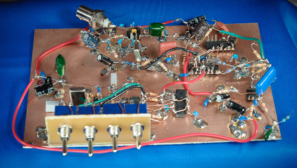
Above — Reference oscillator, offset mixer and PLL circuitry all on 1 very ugly board.

Above — Bench photograph of the reference and offset mixer breadboards in place and under test.

Above — Another view of everything but the VCO.
Conclusion
PLL math and theory proves interesting. PLLs are often simple-looking circuits that hide enormous design problems to solve when you dig deeper; especially when you need a low phase noise synthesizer. Still, too, when they work, then it's the happy dance.
My thanks To Wes, Ken, Matjaž Vidmar and the many PLL authors for inspiration and knowledge sharing. I look forward to making some VHF to UHF PLL circuitry to listen to galactic noise in the future.
Out Takes
Prior to learning how to design PLLs, I would have built a frequency stable Jupiter receiver local oscillator by mixing 2 crystal oscillators and tuning 1 or both. I actually built 1 in on a Saturday afternoon November 2014 and show the circuitry more for a lark than anything else. This LO proved a lot of work -- and for me at least, it's easier and better to make the PLL version.

Above — Jupiter oscillator with variable tuning by a front panel cap. To garner greater frequency swing, I applied two 25 MHz crystals in the "super VXO" format. The tuning range was only 20.52 to 21.146 MHz. Lacking any Gilbert cell mixers like the NE612 at the time, I plied a diode ring mixer.

Above — The triple tuned filter that follows the mixer + simple diplexer. IL = 3.4 dB.

Above — The final amplifier that follows the triple tuned filter output. I was going for strong reverse isolation.

Above — The entire breadboard in a die cast enclosure.


Above — The VXO breadboard with temporary BNC port for testing.
Links
Here's a link to some Jupiter radio receivers along with software and technical material: Click
beautiful work, congratulations !!
ReplyDeleteI continue to admire your devotion to the art and science of radio, as well as the amount of effort that you put into learning new topics. Very impressive work as always!
ReplyDeleteBravo. thanks
ReplyDeleteVasily,
ReplyDeleteyour breadboard is not ugly. It is beautiful with careful attention to layout, short leads and general respect for RF. Having made many a circuit like this including ECL-based 500+ MHz VCO, encoder and decoder. Chip resistors and capacitors work even better. I like your phase detector and VCO!
Thanks
ReplyDeleteExcellent write-up and execution of principles! And.....my building style: deadbug. LOVE IT! It works and its easy to work on and modify to "make it work" from basic modeled principles.
ReplyDeletePhase noise is something that totally escapes the newbie and even the suppliers of commercial single-chip PLLs. I was once called in to "solve" a jitter problem in a large distributed storage installation. Spectrum analyzer and decoupling capacitors in hand, I connected to the master PLL in the system to the spectrum analyzer. Yea,.....sure,....-8 dBc to the beginning of the noise pedestal! My recommendations: first understand phase locked loops at the basic (discrete) level. Then go to your suppliers and require a low phase noise design. You might have to educate them on how (simply) to measure phase noise.
Nuts. Didn't know I had to sign in for ID to be posted. The last post commenting about phase noise was by
ReplyDeleteDave Eckhardt - WØLEV
dobra.thanks eduardo
ReplyDeleteNice work and idea all constraction...
ReplyDeleteIn fact a PLL system has a PI controller. P stands for Proportional, I stands for Integrating.
ReplyDeleteWe have followed you since 2004.Thanks Thanks Thanks
ReplyDeleteDel Pearson. ^^ SWL, Arduino, GPS, and radio astonomy
Привет,
ReplyDeleteНе могу найти ваш приемник прямого преобразования на 7мгц.
Не подскажите где посмотреть.
Вы думаю, лучший кого я видел в интернете.
Спасибо.
Александр.
ReplyDeleteСпасибо Александр
На моем блоге --- http://qrp-popcorn.blogspot.ca/search/label/Funster%20receiver%20Part%201