Search This Blog

Wednesday 29 October 2014

Harmonic VXO


Greetings:

I needed a quick, very temperature + frequency stable oscillator @ 50.8 MHz to test a receive mixer. Already running elsewhere on my bench, my main VHF signal generator wasn't an option.

Without going to a digital signal box, I weighed my build options:

  • VFO — difficult to stabilize at VHF.
  • VCO — even more difficult to stabilize at VHF and it's too much work to make a PLL for it.
  • Overtone crystal oscillator — little chance of finding a crystal to vibrate at 50.8 MHz.
  • Fixed crystal oscillator  — need a crystal to vibrate at exactly 50.8 MHz. Right!
  • VXO  — do I own a 10.16, 16.93 , 25.4 MHz etc. crystal ?
  • VXCO — still need a crystal to double, or take a harmonic from. The varactor will add phase noise, but might work.

Then came a mad search. Soon enough, I found a long forgotten bag of crystals and after 10 minutes of fumbling with it, I felt jubilant to find a 16.9344 MHz crystal!  Good, I'll make a VXO with an output filter to help suppress all but the 3rd harmonic.

I grabbed a copper board and began soldering — no need for a schematic, for I've made many tens of xtal oscillators in my sleep. About 20 minutes later, I was done and ready to measure the ugly thing.

Breadboard

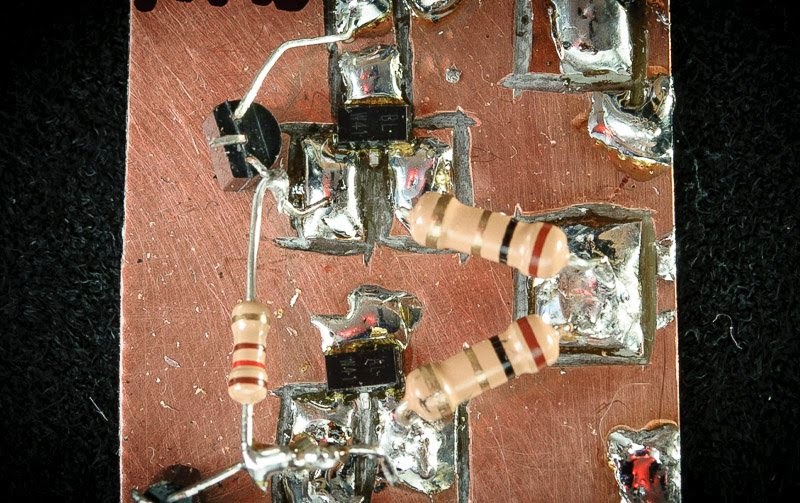
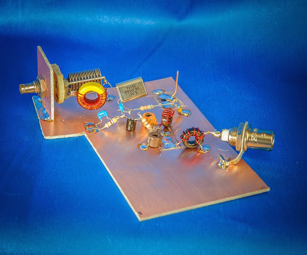
At ~50 MHz, I foolishly went with single-sided Cu board and apart from a couple of carved squares, built with super-fast, classique Ugly Construction. The yellow toroid core = a T50-6, while the black parts are T37-10 powdered-iron cores. Low cost, low Q, garbage-grade trimmer caps employed.

A harmonic fixed xtal oscillator come VXO

Above — A harmonic fixed xtal oscillator come VXO. First I ensured that the 16.9344 MHz was indeed a fundamental crystal by shorting the transistor's collector coil and measuring with a 10X probe ---- DSO with a built in frequency counter.

The doubled-tuned circuit values were chosen based upon my work with 6 Meter band-pass filters 2 years ago. As I recall, the 3 dB bandwidth is around 1.8 MHz for ~250 nH inductors, a tuning capacitance around 31 pF and a 1 pF coupling cap between the resonators.

I build progressively: First made a fixed crystal oscillator and then after tuning up the output filter, measuring DC + AC voltages and current, I then added the VXO parts shown below the red arrow. The 3.8 µH inductor was just something lying in my #6 material toroid parts drawer.

I keep several pre-wound inductors in each size hand to speed up design work. All I have to do is remove a few turns as needed, or go to a toroid that looks like it contains more wire. I don't count turns except when making transformers and instead rely on an LC meter to measure the inductance.

Spectrum analysis after tuning the VXO for ~50.8 MHz

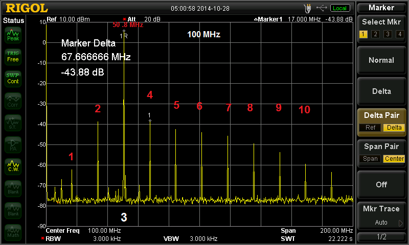
Above — Spectrum analysis after tuning the VXO for ~50.8 MHz.  I red numbered the tones starting at the crystal's fundamental frequency. The strongest harmonic = the 4th tone @67.6 MHz lying  -43.9 dBc.

The VXO  output in time domain

Above — the VXO output in time domain.

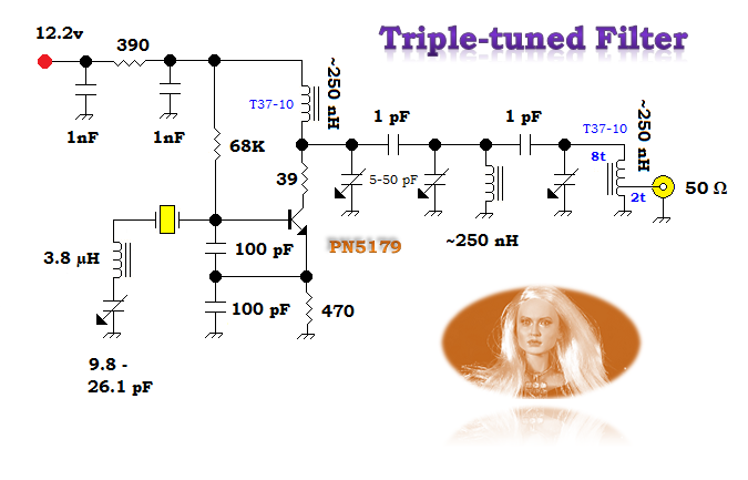
A triple tuned version.

Above — A triple tuned version.

The double tuned version contained too much harmonic energy, so I added another identical tank and re-measured.

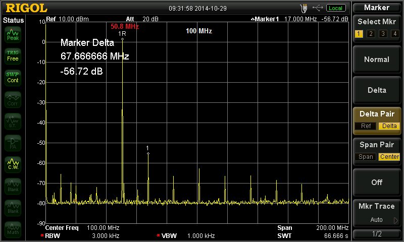
Spectrum analysis of the TT harmonic VXO.

Above — Spectrum analysis of the TT harmonic VXO. Strongest tone = -56.7 dBc; most are under 63 dB down.

Now that's what I'm talking about!  Onto my mixer experiments...

73,  V/T

Friday 24 October 2014

Funster Receiver Notes Part 3

Funster Receiver Notes Part 3
Audio PA, side tone and wrap-up.

The most common home brew receiver part = the LM386 audio amplifier.  A Signetics brainchild like the NE/SA602, the LM386 first appeared in home brew receivers in the late 1970s. The impact of the Signetics design team on modern home brew radio building exemplifies an outward phenomenon.

Although, I too occasionally drive speakers with the old 386, distortion develops at just ~300 mW average power and nobody's ever called it a low-noise part; especially when the internal gain is set higher than 20.

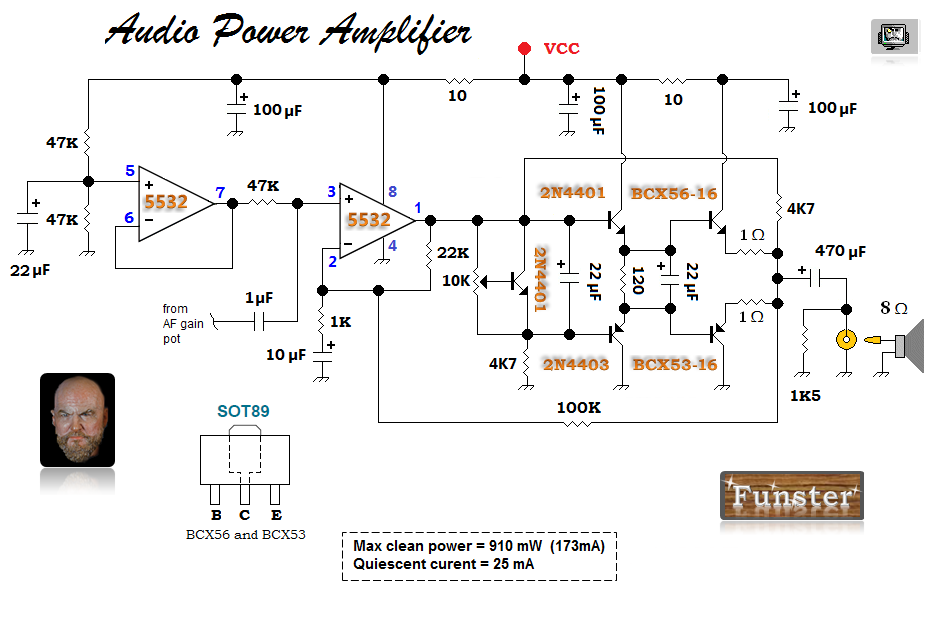
For years, I've plodded to find a popcorn discrete replacement for the LM386. In the Funster receiver, I evolved my basic popcorn AF PA design a little more — it still needs work, but I can look you in the eye and tell you that Funster sounds great and exhibits low AF chain noise.

My earlier popcorn AF power amps ran low voltage gain and I didn't realize this was a problem until readers emailed to say so. I get it now — in our RF home brew community some expect the full-on gain (200) of the LM386!  In contrast, when I run a 386, I set a gain of 20-50. Talk about different perspectives. That's what makes home brew RF design exciting.

Popcorn Audio Power Amplifier


My first popcorn AF stage with a 5532 non-inverting amplifier

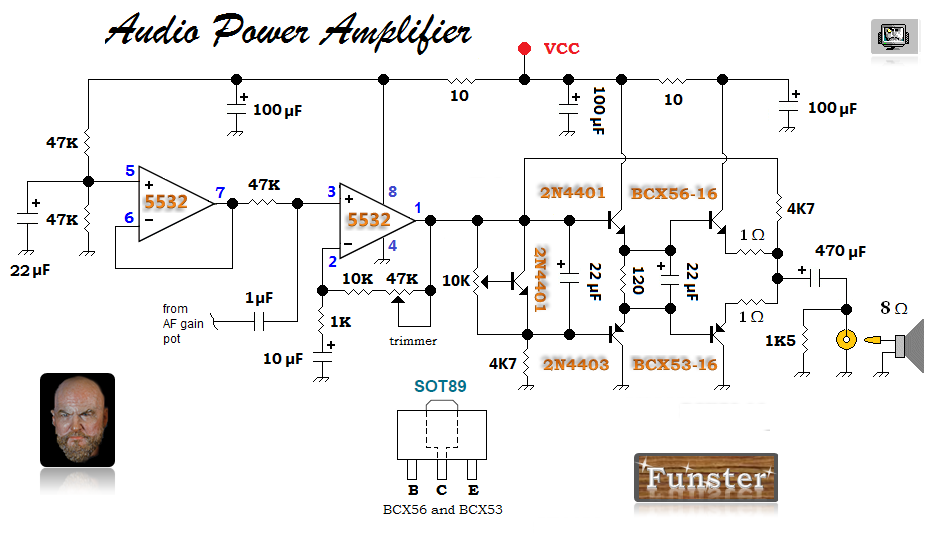
Above — My base popcorn AF stage with a 5532 non-inverting amplifier features adjustable gain to appease builders who rely on the PA stage for most of their voltage gain. You may change the fixed and/or trimmer series resistors between pins 1 and 2 to set your desired gain either by listening to your receiver, or crunching some op-amp arithmetic [ Vo = Vin (1 + R2/R1) ]. I fixed the other half of the 5532 op-amp as a voltage follower / rail splitter.

The 2 power followers pairs are biased into Class AB by a 2N4401 level shifter. Tweaking the 10K trimmer pot even the slightest may change your idling or quiescent current dramatically; so carefully set the bias with your test equipment switched on.

I wrote a web page on biasing your AF finals: 2006 - 2009: Complimentary Symmetry Amplifier Biasing Basics.  You'll find it in the Old Site archive. A quick review follows:


Measuring quiescent current + the voltage dropped across both NPN/PNP power follower bases.
 
Above — Measuring quiescent current + the DC voltage dropped across both NPN/PNP power follower bases. Typical popcorn AF amplifier values are shown. In most cases, you'll measure 1.1 to 1.4 VDC across the final pair with properly set bias. 

I set the final amplifier pair bias in the popcorn AF stage just like I used to with 100 watt guitar amplifiers: put an appropriate resistive load on the output, connect a signal generator to the input and tweak a pot to find the set point where the crossover distortion disappears.

I keep 2 DMMs on my bench: 1 serves exclusively for power measurement and I never fire up a "just built" power amplifier stage of any sort without an ammeter connected between the DC power supply and VCC point.  I only want to enjoy my measurement experiences — the ammeter will catch any shorts or other problems long before thermal runaway takes out your NPN power transistor (we rarely blow the PNP in a complimentary pair).

With no applied signal, your ammeter will read the quiescent current of your whole PA stage (some purists argue that quiescent current only applies to the final complimentary pair). I usually set the bias and measure my quiescent current after the finals have warmed up. It's best to thermally couple the adjustable NPN level shifter to the PA heat sink, but you may omit this in popcorn-class PA stages.

After setting the bias, switch off the signal source. After that, measure across the 2 BJT pair bases and then look to see what the ammeter shows. Expect 20-35 mA quiescent for a warmed up popcorn amplifier.


Above — Average power measurement and formula. A 1 KHz low distortion signal generator makes a great weekend project — mine feature variable gain Wien bridge oscillators with 2-4 poles of low-pass filtration using extremely low-noise op-amps. Without solid measurement tools we're just bench lackeys.

Back to the popcorn power amp shown earlier: 1 strength is that the sections labelled PA (the 1 µF and all the parts to its right) will add a PA stage to any voltage amp with a low output impedance. 1 weakness = the output is open loop — with no negative feedback to reduce distortion. 

In previous experiments, I left out the PA's 1 µF coupling capacitor plus the 4K7 resistors and just drove the power followers with a DC coupled op-amp output. This works fine for headphone-level output power — but I'm a speaker guy. When driving a speaker loudly during signal peaks, the drive to the followers may poop out and distort the signal with a glitch that resembles crossover distortion. Increasing the quiescent current won't fix the problem — I've tried that.


Above — Distortion viewed when swinging a Vpeak-peak of 7v with DC coupled op-amp drive.

Evolution 1.
Above — Evolution 1. I removed the 1 µF coupling capacitor (good riddance) and arranged the top 4K7 resistor to provide positive feedback. The op-amps were able to drive the followers all the way to normal harmonic clipping with no aforementioned glitch. The bootstrapping also boosted the maximum clean sine wave power.  

Evolution 2. This final PA stage went into my Funster

Above — Evolution 2. This final PA stage went into my Funster. I added a negative feedback loop via a 100 K resistor to put the op-amp into the loop. Do not put a parallel capacitor across the 100K feedback resistor as this will increase distortion in my positive + negative feedback arrangement.

Further, while listening to a variety of CW signals into a speaker. I tweaked the 5532 gain trimmer between Pins 1 and 2 as I adjusted Funster's 500 Ω AF gain pot. When satisfied with the non-inverting amplifier's gain, I removed the trimmer + fixed R between Pins 1 and 2 and measured a series resistance of 21.4K Ω . I soldered in a 22K resistor, retested and felt it gave the prefect amount of PA stage gain for my particular Funster. Let's get to the PA power measures:

The maximum peak-peak voltage of the final Funster PA design into a 8 Ω resistor load = 7.64 Vpp.

Above —The maximum peak-peak voltage of the final Funster PA design into a 8 Ω resistor load = 7.64 Vpeak-peak. To calculate average power we use the peak AC voltage, so divide Vpeak-peak by 2 to get Vpeak. Therefore Vpeak =  3.82v. 

So my clean signal (average) power = 3.82v * 3.82v / 16Ω = 912 mW.

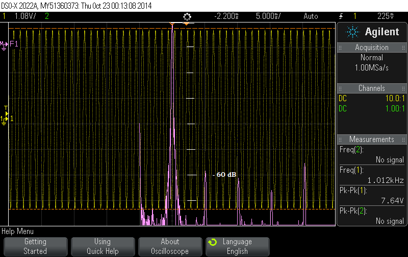
If I increased the drive on my 1KHz signal source any more, the AC signal began to clip. I pushed it just into clipping and then backed off until I eyeballed a pure since wave and got the Vpeak-peak = 7.64 shown above. Admittedly, eyeballing the sine wave feels subjective, however, if you lack a distortion analyzer, a DSO with a good FFT or a sound card/computer audio analysis program, sine wave signal viewing works okay.


Above — The FFT of the sine wave signal above on my DSO showing harmonic tones to the right of the fundamental 1.012 KHz signal. The second harmonic lies 58 dB down indicating my eyeball sine wave assessment works okay. FFT measurement is a better idea though.

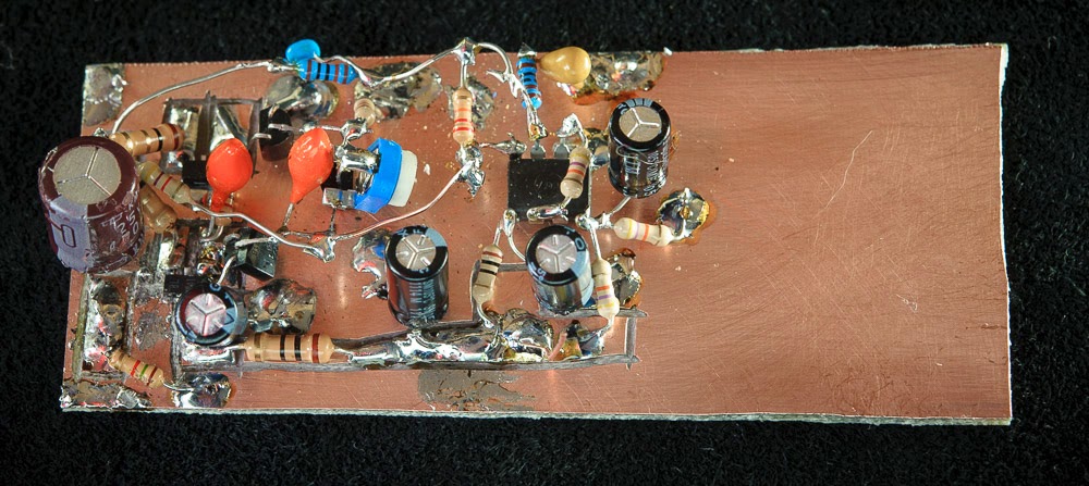
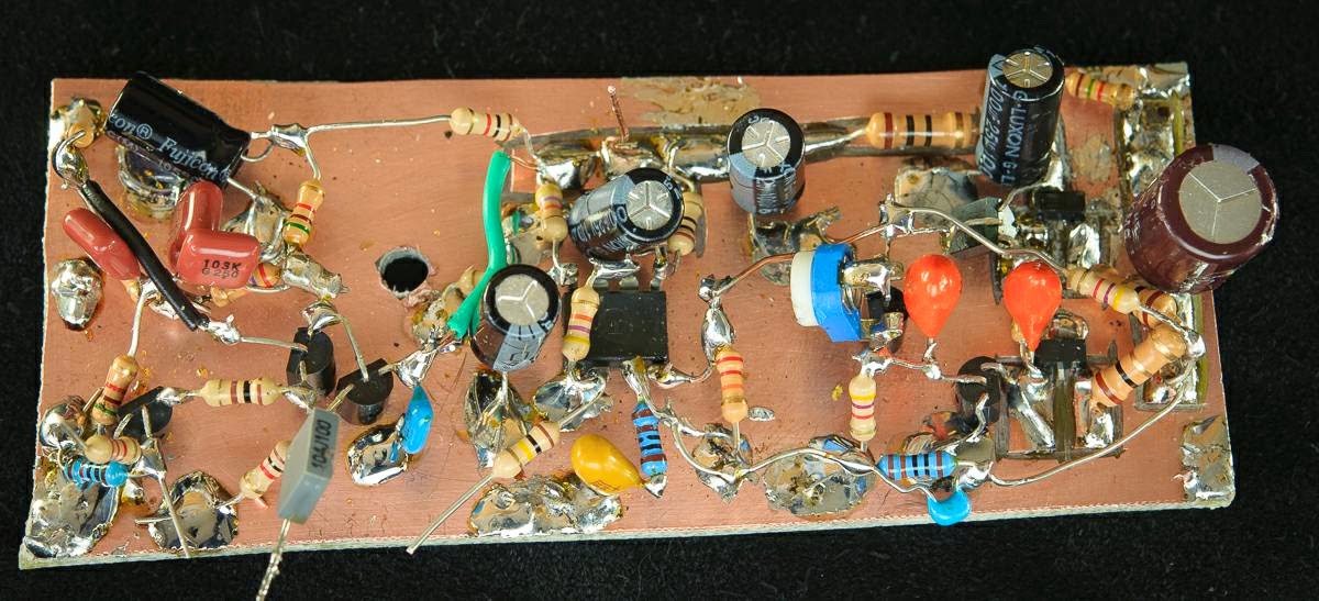
Breadboard of the popcorn AF amp I bolted in the Funster receiver

Above — Breadboard of the final popcorn AF amp I bolted in the Funster receiver. I added temporary RCA jacks and tested it on my workbench by listening to Funster.  A shielded cable temporarily connected the installed tone/mute circuit to the rear panel RCA speaker jack. From the speaker jack I patched a shielded RCA cable to the PA input and connected the PA output to an 8 Ω speaker.

This breadboard shown ran a 220 pF cap across the 100K negative feedback resistor — I promptly clipped it out since the capacitor generated distortion.

I'll keep working on my popcorn AF power amp, but this 1 sounds good in Funster and certainly beats the old 386.

Keyed Side Tone


 Above — A phase shift oscillator circuit sent to me by Wes, W7ZOI awhile ago.

I love Wes' side tone circuits and this sine wave generator combined with the mute circuit sounds makes Funster sound like a professional transceiver as I key the companion Funster transmitter.

For amplitude adjustment, I added the 25K trimmer to get a sine wave in your 'scope. I measured and replaced the trimmer with a nearest standard-value resistor in my final build. Many sine wave AF oscillators don't fare well with downstream changes so I added an emitter follower with 4 mA emitter current + AC coupled a 100K resistor on either side of the 10K volume control.

The 100K resistors, attenuate, isolate and add some low-pass filtration to the side tone output. The last 100K R connects to Pin 3 of the 5532 in the PA.

To "key" the circuit, ground the cold end of the 100 Ω resistor with some solid state switch or a key if you want to use this as a stand-alone code practice oscillator. For the latter, don't forget to add some key shaping to remove bounce-bounce clicks. Lacking the correct part, I substituted a 0.27 µF polyester cap for the 0.22 µF called for in the schematic and still pulled off a low distortion sine wave @ ~782 Hz.  


  Above — The side tone signal in my DSO measured with a 10X probe.

AF stage breadboard with the side tone circuit added.

Above — AF stage breadboard with the side tone circuit added.

Wrap-up

The Funster proves a relatively-simple DC receiver offering significant improvement over the standard direct conversion receiver with no opposite sideband suppression. It compares well to the classic superheterodyne receiver that employed a single crystal filter plus front panel phasing control to provide a single, deep notch on the opposite sideband.

As ever, by the time I complete a radio, I would have made it differently. Ours is a hobby where we make our circuits better over time with our test equipment switched on.

Funster Photos (click on the photos to magnify as usual)

Funster Receiver 2014


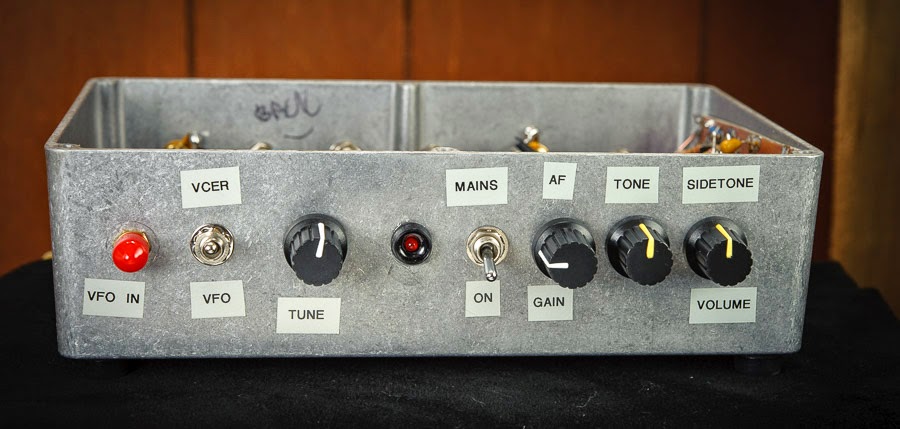
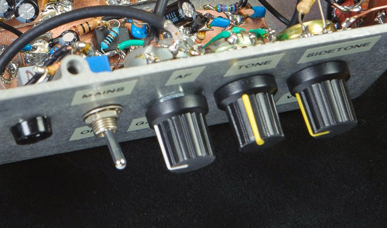
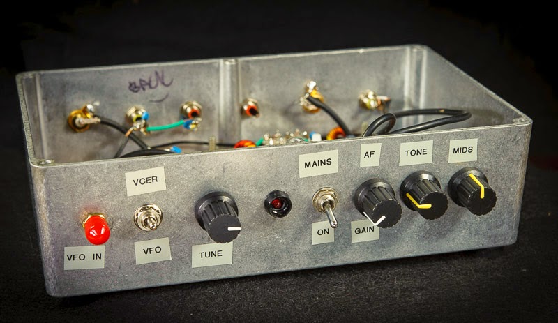
Funster Receiver 2014 --- front view


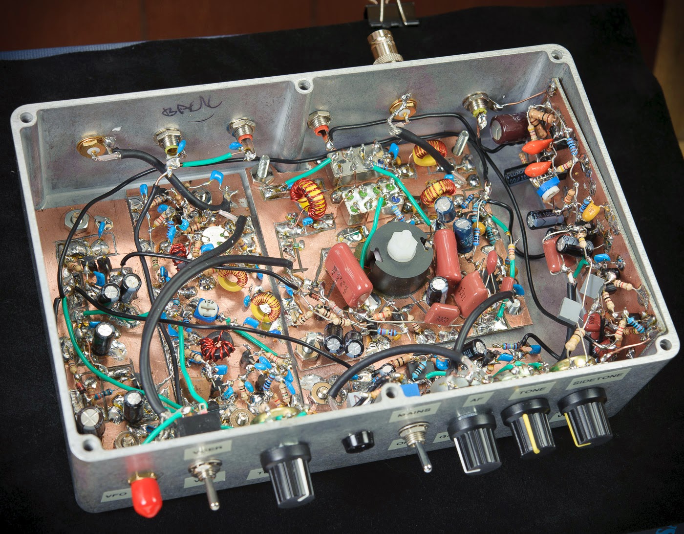
Funster Receiver 2014 --- top view


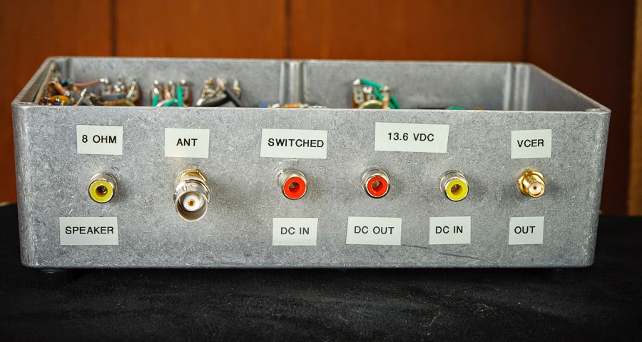
Funster Receiver 2014 --- rear view


A close-up of the NXP BCX56 + BCX53 mounted in a prototype PA board


Above — A close-up of the NXP BCX56 + BCX53 mounted in a prototype PA board. I ran no heat sink other than PC board traces for the collectors. A better choice might be the related BCP56 + BCP53 pair in SOT223 since the bigger package of this BJT pair better sinks heat.
A good through hole substitute = the BD139/140 complimentary pair.

Большое спасибо to all of my mentors and helpers for your support in addition to the 2 workbench companions shown below:

The girlz


Click for Funster Part 1

Click for Funster Part 2
Sunday 19 October 2014

Funster Receiver Notes Part 2
Funster Receiver Notes Part 2
RF front end, AF preamplifier, tone control and mute. 


The block diagram of Part 2 Topics

Above — The block diagram of Part 2 Topics.

40 Meter CW Front End

Welcome to part 2 — the Funster receiver front end arose from my experiments with Chapter 9 of Experimental Methods in RF Design EMRFD
Front end

 Above — All passive front end schematic.

In EMRFD and his QST R2 and A Binaural I-Q Receiver articles, Rick, KK7B vividly wrote how to design in-phase splitters and RF quadrature hybrids, so I won't go into detail.

My RF and AF quadrature hybrid center frequencies = 7.04 MHz and 723 Hertz respectively. To calculate the correct
L and C values, crunch the familiar formula L =  desired Ω / (6.28 x frequency in Hz). So for the 50 Ω RF quad hybrid inductor:  50 Ω / (6.28 x 7040000 Hz) = 1.13 µH. To calculate the companion capacitor value in pF:  C = 1 / (6.28 x Frequency in MHz x desired Ω) C= 226 pF, but we normally substitute the nearest standard value: 220 pF.

The audio phase shifter L C components are nearly the same raw values — but scaled up for AF.

I ran 2 SBL-1 diode ring mixers (DRM). Some gasp at their price, but I bought them long ago for a song. It's now cheaper to buy surface mount DRMs, or perhaps you might home brew some?  If you make your diode rings with SMD Schottky diodes, with any luck you'll find some with 2 diodes per chip, or even better — in a quad ring for strong matching. For example, last year I built a lovely VHF-UHF DRM with the quad HSMS-2827 part in SOT-143. 1N4148s can work okay for HF: most builders rummage through their collection and use the 4 that have the closest DC forward voltage drop.

In keeping with the "20 dB or so" sideband suppression theme of this receiver, I omitted an AF diplexer which helps boost opposite sideband suppression by mitigating mixer output port mismatches. Instead, I just terminated the mixers at HF with the shunt 0.1 µF + 51 Ω R C network and the well matched input impedance of my AF preamplifier.

Far from trivial, it took me 4 tries at winding pot core mH inductors to make a decent 11 mH AF quadrature hybrid. I put the bobbin over  a vice-held pencil (with a thin layer of tape to hold the bobbin firmly) and wound 28 AWG wire from left to right then right to left (and so on)  to make a tightly wound, even coil. I didn't measure, but probably have 487 cm of wire folded in half to make my bifilar coil.


Above — Front end breadboard with a mistake in the 1st quadrature hybrid.

After I photographed this board, I then realized that I didn't made the RF quadrature hybrid with a bifilar wound single toroid! Showing this photograph keeps me humble and besides, I don't have any others photos of the passive front end to show.

This receiver front end shows but 1 method to make a DC receiver with 20 dB or so sideband suppression.  Many readers wrote to tell me about other phasing methods such as the exciting Tayloe system — thanks guys!

While I could find many examples of phasing rigs using CMOS switches/all-pass op-amps etc., this is the only rig I've seen based on EMRFD Chapter 9 experiments other than the R2 and binaural receiver also published in QST by Rick, KK7B.

To clarify. My blog records the work of a lay-person as I bumble along trying to learn about radio electronics design. It's just 1 warts-and-all viewpoint and not a comprehensive guide to what's 'out there' by any means. I enjoy the many perspectives shared about radio topics and just offer my 2 cents worth.

AF Preamplifier


AF Preamp Chain

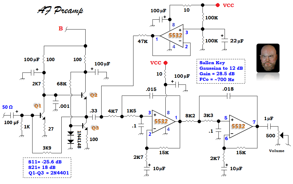
Above — AF preamplifier chain schematic with measures.

With all of the receiver gain at AF, I sought a low noise preamplifier chain. After testing many designs, this 1 jumped out. The strong input return loss [25.6 dB] makes it suitable to follow any diode ring mixer product detector.

Q1-Q3 realized my goals of swinging the biggest possible AC signal without adding much noise while obtaining a 50 Ω input impedance and a low output impedance. Q1 and Q2 form a shunt feedback pair that offers wide band AC and DC stability. Because the shunt feedback from the emitter of Q2 to the base of Q1 lowers Q1's input impedance greatly, I needed to add the 27 Ω resistor for emitter degeneration (series feedback) to bring the Q1 input impedance up to 50 Ω. I made the return loss measurement with my home brew 50 Ω AF return loss bridge documented in my old website archives.

Q2 features a current source output (Q3) to boost its load driving capacity. The output 0.33 µF
capacitor rolls off AF < 100 Hz or so. All the AF signal chain capacitors should be "polysomething" as possible.  A 1 nF cap on the Q1 collector bypasses any higher frequency RF to ground.

5532 op-amps represent an amazing performance per cost ratio and 2 years ago, a retired EE from the Midwestern USA sent me 25, and so, I've been working on those parts for awhile. Thanks Scott! 

An op-amp splits the VCC and delivers the 1/2 VCC virtual ground via a 47K resistor. The 47K contributes nearly zero noise because the low output impedance of the first preamp is in shunt with it. The 47K decoupler R is required because without it, the near zero output resistance of the 1/2 VCC op-amp would hugely load the BJT preamp.
2 op-amps deliver gain plus low-pass filtration via 2nd order negative feedback filters. The impedance of the feedback circuit decreases as frequency increases, thus the closed-loop gain runs highest around the lowest frequency.

With a 700 Hz cutoff frequency, clearly this receiver is set for CW reception. It's best to design your own filters and TI offers a great free program called FilterPro that I've enjoyed for years. I also experimented with some of the cap values: for example changing the 0.15 µF cap in the first op-amp to 0.22 µF will make the filter howl, Although the design called for 0.20 µF in that slot, I preferred 0.15 µF.

AF preamplifier breadboard on the front end board

Above — AF preamplifier breadboard on the front end board.

I really had to cram the AF preamplifier guts on the copper board, however, this is the natural outcome of designing while you build. 

I also took the time to review op-amp theory. Op-amps are about as "black box" as it gets for us. Clear, well documented math guides their use and so it's possible to design with calculations or software and then actualize precise results on your bench!  A few years ago, I built discrete component op-amps to learn more about them. While my designs suffered from questionable noise performance, the math worked and I felt vindicated. Ken Kuhn in "My Links" offers super op-amp tutorials, although many are high level. You'll find numerous other op-amp tutorials online.


Above  A discrete "op-amp" for experiments.

For those inclined to go further, Ken Kuhn sent me this high gain JFET inverting amplifier for my discrete op-amp negative feedback experiments — the open loop gain ranges from many 10s to over 100. Set bias (RE1, RE2) so that voltage at emitter of Q3 is roughly 2/3 VCC.  This circuit uses DC feedback for bias stability.

All inverting amplifiers with an input resistor (RB) will generally suffer higher noise because of the noise voltage of RB. For high level circuits this is of little if any consequence. For low-level circuits it could be a major factor. Regardless, it's good for learning.

A 500 Ω volume pot controls the AF gain — from the datasheet, that's the maximum load we should apply to the 5532 output to maintain proper distortion performance. Following that, I ran a single knob tone balance circuit with a mute circuit cobbled to it.

Tone Balance and Mute Circuitry   


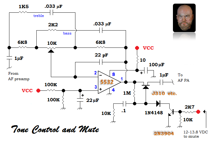
Tone balance and mute schematics

Above — Tone balance and mute schematics.  I show this tone circuit with permission of its designer, Douglas Self. 

Amateur radio receiver manufactures fill their receivers with interference fighting tools and it's rare to see standard tone shaping circuitry. This also trickled into our home brew receiver practices. 

I'm not sure whether you'll like or want a tone circuit, but I do. At 1 end of my radio circuit chain lays an antenna and at the other, a speaker. Salty old radiophiles tell us it's best spend your hard earned money on your antenna system to boost performance; while learned audiophiles carefully choose and equalize their often expensive speakers. My speakers are also well chosen, cabinet mounted and I like tone control(s) to tweak the sound for whatever speaker and room (or tent) I'm listening in.

The tone balance control came from an amazing book called Small Signal Audio Design: 2nd edition. Douglas Self, a recognized audio design authority writes beautiful, fun to read prose and his book ranks in my top 5 because it offers unassailable knowledge + inspires and teaches me how to write better. In short — insightful + actionable info for the DIY builder.

My sincere thanks to Douglas for his work and for giving me permission to show this circuit.

Tone and mute circuit breadboard

Above — Tone balance and mute circuit breadboard. I soldered in a temporary pot + input/output RCA lacks and tested the circuit before installing it. As mentioned in Part 1, I ran a temporary shielded cable from the 500 Ω pot output to an RCA jack on the back of my receiver. Thus I could easily test my tone and AF power amp circuits ex situ.
A close up of the tone and mute circuitry

Above — A close up of the tone and mute circuitry. I carved 4 pads in the copper clad board: 1 for Pin 1. Another for Pin 2 + the wiper and then 2 more as solder points for the left and right potentiometer terminals. The 6K8 resistors were size 1206 SM parts. I changed 1 resistor from the original by D. Self: the 1K5 R was 2K2 in his book. Further, I converted it to single supply.

A 100K resistor connects Pin 5 (+) and 6 (-) of the unused half of the 5532 to 1/2 VCC.

Douglas Self adapted and modernized the tone balance control originally published in Wireless World for March 1970 by R. Ambler. This circuit often referred to as the Tilt or Ambler never really caught on mainstream, however a version got famous in the Quad 34 amplifier. As it boosts the bass, it cuts the treble and so forth. Although I tried a traditional bass/treble Baxandall design, the tone balance control won my favor in this receiver and happily it adds very little noise.

Uncertain if I really liked it [was I just practicing gimmickry?] — I listened without it for 2 nights and then for 2 nights with the circuit inline. I preferred running the tone balance control because it adds a little sizzle back into my AF chain when listening in my radio room with my tuned, ported speaker. Your experiments may find otherwise.

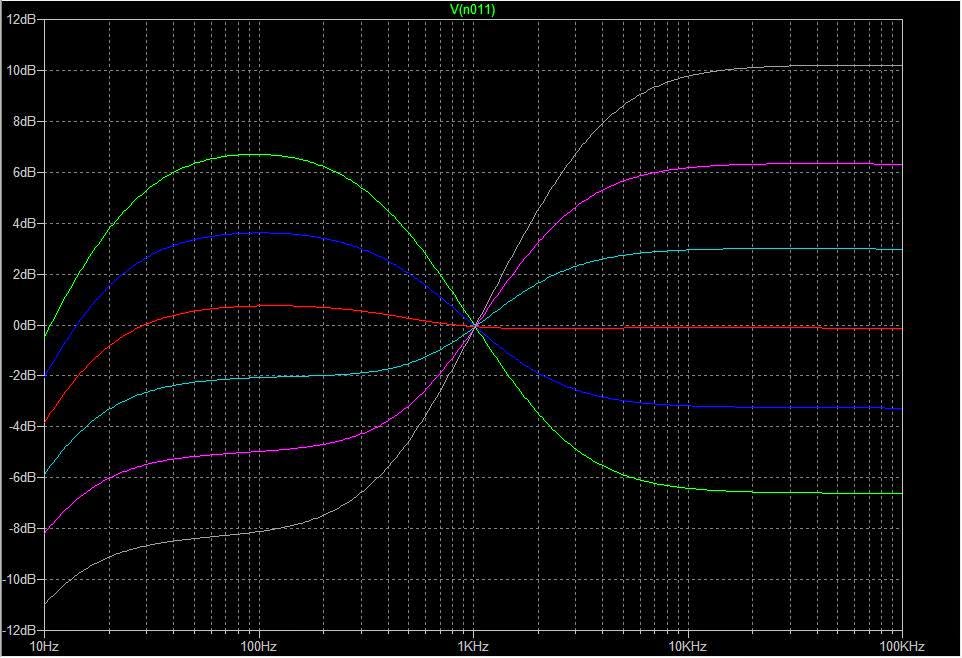
A SPICE plot of my particular circuit

Above — A SPICE plot of my particular circuit made by Victor, 4Z4ME

Thanks to Victor, 4Z4ME who plotted a transfer function with 20% steps of the 10K potentiometer. The mute circuit, my favorite, silently interrupts the signal path when the cathode of the 1N4148 diode gets short circuited to ground. A back panel switched 12v Funster line delivers 12 VDC when the companion Funster transmitter is keyed. Thus a 2N3904 switch grounds the 1N4148 diode to mute the preamp.

Tests show that although a pull up resistor on the 2N3904 collector wouldn't hurt, it's not needed and works fine as shown. Douglas Self also shows some stellar AF mute circuits in his aforementioned book.

In Part 3, I'll show the AF power stage + side tone, plus some odds and ends to wrap up the Funster presentation.

Thanks for reading....

Click for Installment 3


Wednesday 15 October 2014

Funster Receiver Notes Part 1

Funster Receiver Notes Part 1
Part 1 describes the DC control circuits + the built-in, switched local oscillator.


Preface

The Funster serves as fodder for your own experiments. The front-end RF concepts and bifilar wound quadrature hybrids come right out of EMRFD Chapter 9, however, in no way does Funster come close to perfection. By the time you read this, I'll have changed something.

In context, I enjoy this excerpt from Rick, KK7B taken from a technical file he posted about common gate JFETs. He wrote this after related discussions on the Yahoo EMRFD Discussion group and from questions by his students: Note: Rick refers to his schematics as public domain art.
 
“For art, the time honored method is continuing study of other people’s work and practice on your own creations. You will get better with time. Your 20th project will look better and work better than your first or second, so it is critical that you get off the simulator and get to the bench and start building and measuring your designs”.

Block Diagram


Above — block diagram for the DC & oscillator circuits.

DC Circuitry

Before building Bob, K3NHI’s utility sweep generator in 2012, I gave lax importance to the DC circuity in my home brew works.  Bob's clinical approach awakened me! Thorough and passionate; with no patience for mysticism, Bob imbues that from DC to daylight, solid physics, measures and practices affirm every board in a successful project. Kopski’s law: To measure is to know became my mantra.  Also, since then, my DC control circuits get front row attention — I now build them on their own little board with due care. They're fun too!

We need good role models in all things — including QRP home brew. With social media, poor practices and innocent circuit or drafting errors may get widely adopted after the mere click of a mouse. We all make mistakes (me more than most), so please discern carefully and measure whatever you can, whenever possible. Your measures might teach you more than someones words or photos.


Above — The DC circuitry to power the various stages.

A Darlington capacitance multiplier circuit low-pass filters noise riding on the first AF preamplifier DC line. The base connected 100 µF cap gets multiplied by the transistor current gain. I hear 0 hum.

A zener diode voltage regulator for the built-in LO copies a design taken from the TNT web site with measures showing it reduces zener diode noise. The front panel mounted 10K pot tunes the built-in variable frequency ceramic oscillator [VCER].

S2 is a front panel DPDT that switches between an external VFO, or the built-in local oscillator along with its DC power supply. Buffers 1 and 2 draw lots of current, so it's nice to switch them off when they're unneeded. I designed + tested all circuitry with a home brew 13.6 VDC power supply, but use various DC supplies in the field.


Above — An early photo of the DC circuit breadboard

Although unseen, I measured voltage and as appropriate, the current in all my circuits to ensure proper function and to get au fait. Over time, I've learned what to expect and to stay in "debug mode" throughout the design/build process. Some examples: the zener diode regulator output measured 9.34v with a temporary 1K5 resistor load and the Darlington capacitance multiplier circuit drops the DC by 2 base-emitter junctions, or a 1.2v drop when loaded with a temporary shunt resistor to test it.

Popcorn QRP is not about making radios. Making RF and audio circuits merely veils our real intention — to joyously measure with our test equipment, learn, share and get better at it. To delight, surprise and illuminate each other through a considered approach — now that's home brew radio! Gosh, don't try to talk to me into making various PC boards. They're often just a creative straight jacket making us conform to mediocrity, or at the very least, to someone else's vision. Go your own way if you can.

Built-in Local Oscillator

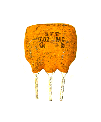
A nice guy called Peter, VE3GYY sent me some Murata 7.020 MHz ceramic resonators some years ago.  For those of you who send me free parts, have faith — I'll eventually put them in a circuit and really appreciate your support.

Above — 1 of 4 ceramic 7.02 MHz oscillators I own.

Considered a poor man's crystal, ceramic oscillators are cheap to produce and serve as clock sources for all sorts of commercial digital gadgets. Sadly, it's hard to find them resonant on the Ham bands. Peter also sent this website as a reference. He also will sell them to you for low cost. Please email me or see the comments section of this blog page. My 4 varied widely; but with a 400 pF air-variable capacitor and a Colpitt's oscillator , I pulled them all 35-40 Hz right down to the bottom of the 40 Meter Ham band. A 40 Hz delta F = fun times. I measured a Q of ~ 1200, so phase noise performance suffers compared to a crystal. They're no panacea. I found mine prone to self-oscillation.


 Above — My internal ceramic oscillator (VCER) and 1st buffer.

Although a VXO might have worked, at 7 MHz, the delta F runs quite low, so I went with the
VCER circuit shown. Since the output contains a lot of harmonics, I designed and built a low-pass output filter to mop up distortion. Even with the 10K hycas trimmer pot cranked to give maximum gain, the output was only ~0 dBm, so a 2nd buffer follows.

The trim pot allows me to set 11 dBm power exiting the second buffer — this gets reduced to 7 dBm by a 4 dB pad on the LO input of the RF front-end board. I can deliver up to 10 dBm to the quadrature hybrid driving the mixers if wanted. I'll show the front end and small signal AF circuitry in Funster Receiver Notes, Part 2.

Because I lacked room in my chassis, voltage tuning provided my only option. I spent many hours trying different schemes + parts and settled on two MV2105 varactors. Varactor tuning seems foolish since it degrades LO phase noise and temperature stability, however, for high performance reception, I can switch the Funster's image-reject mixer with an external, high quality VFO. The VCER works great for casual tuning and ragchewing.

A 1K resistor between the 10K tuning pot and ground keeps about 0.8 reverse DC on the varactors at the maximum frequency — without applied reverse DC at all times, the VCER will shoot up to 7.2 MHz or so.
Although the varactor DC line 0.1µF bypass capacitors are shown on the DC control board, we need to AC bypass immediately next to the cold side of the 100K isolation resistor (at Point D above) to prevent parasitic oscillations. This is true of any varactor DC control wire decoupled by a resistor or choke.

Experimental as can be, the VCER circuitry results won't be reproducible and I show it for interest sake. Ceramic resonator frequency stability lays somewhere in between a VFO and VXO.  I can listen to a 20 minute QSO without retuning when the frequency is  <=7.039 MHz. Above 7.039 MHz, a slow, downward drift becomes noticeable.


 Above — My VCER 2nd buffer and external input/output.

A 2N5109 feedback amp gives needed gain plus a well-defined output impedance that's further boosted with a 3 dB pad. A high return loss is essential when driving diode ring mixers and a  another unseen 4 dB pad on the LO port of the quadrature hybrid helps reduce the mismatch caused by S2.

Some VCER signal gets stolen by a 18 pF series capacitor and then buffered/amplified by a common base/common emitter cascade. This scheme provides a well isolated, low impedance external port for connecting a frequency counter. The output @ ~2.7 dBm (shown below in green) is not quite linear because I kept the current under 16 mA with the 560 Ω emitter resistor on the emitter follower. Increasing the follower's emitter current may give linear output; so will reducing the 18 pF capacitor to reduce input drive. For frequency counting, it works fine. These basic measurements are easily performed with a 'scope and ammeter and in a future blog post, I'll go into that buffer's design.


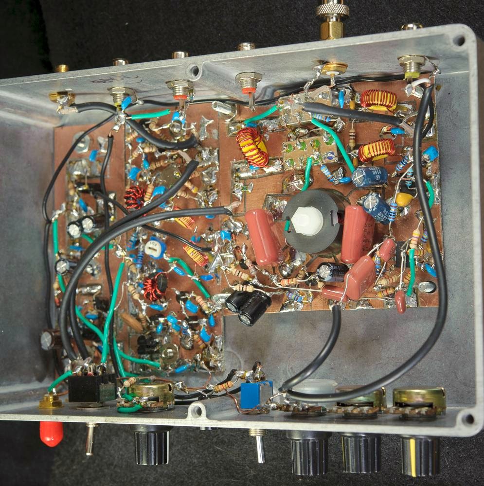
Above — Funster DC and oscillator boards installed [left]. The front-end RF board and AF preamplifier lay on the big square board, although the AF is temporarily routed through a 500 Ω volume pot to what eventually will be the speaker jack — i.e. it's in AF preamp test mode. I connected my lab AF power amp + speaker and listened to it for a couple of nights. As ever, I love DC receiver audio!


Above — LO up close. A high parts density and Ugly Construction make it look messy. [Unlike brave Dave, I don't make pretty gear]. I used a lot of 0.1 µF cap as stand offs and don't trim some of the excess resistor leads until I'm 100% done. The two TO-92 parts = the varactors with their cathodes mounted in a carved island. A few SMD parts adorn this board.


In installment 2, I'll show the RF and AF circuitry up to the audio PA. Thanks for reading.


Monday 13 October 2014

Simpler Single-Signal Direct Conversion Receivers


Greetings!
I love the sonic impact of a well-designed direct conversion receiver. My best, a version of Rick Campbell’s R1 receiver with a Level 17 diode ring mixer still thrills me to bits. How do I describe the sound of a well-designed DC receiver?  Well, subjectively of course:  pure, raw, sibilant and dynamic come to mind. For contrast, after listening to 1 of my DC receivers, I’ll fire up 1 of those quotidian home brew superheterodyne receivers [NE612 — Cohn crystal filter — LM386 etc.] To my ears at least, the latter sounds cadaverous.

The story didn’t end with the R1, for Rick crunched the math, made careful experiments and raised the bar with his follow-on; the R2 which contained an image-reject mixer.  His work ushered high performance, single-signal DC receivers onto the modern day radio workbench with wide-reaching impact.

For image-reject receivers, instead of 1 baseband signal from a DC receiver, we get 2 baseband signals: Q or quadrature-phase that lies 90° out of phase with the I or in-phase signal (phase 0).

Modern DSP experimenters process the I and Q basebands with software, while the more primitive radio experimenter applies analog signal processing — usually some audio phase-shift networks and a combiner to reject 1 sideband before some more AF filtering/amplifying to drive a speaker or phones. Your brain also provides some neurolog signal processing.

The math and design of image suppression receivers gets difficult for some, but for those of you who like math — feast away since web articles abound!  I recommend you read Chapter 9 of EMRFD (written by Rick) — a chapter that offers telling insight for both the electrical/computer engineer and weekend QRP homebuilder alike.


Receivers with Image Rejection of 20-30 dB

Image rejection gets trashed when phase error or gain mismatch occurs in the I and Q channels and reducing these errors takes work. Above 20-30 dB rejection, design and often bench practices become more critical. For example, the audio phase shift networks are typically all-pass circuits with 1% or less tolerance parts built around 5532 or quieter op-amps. 

Further, to extract maximum sideband rejection, tweaks like a phase trimmer and amplitude balance control become vital.

I plan to experiment with image–reject DC receivers with 20 or so dB sideband rejection. This allows us to apply less stringent 2nd order transistor, op-amp, or pot core-based LC phase shift networks, however, receiver design remains a challenge.

Although an audio spectrum analyzer will help, the brain + ears = the main tools we'll use to assess sideband suppression.
Another gimme = no worrying about crystal filters, or an image with a zero IF!

I plan 2 receiver experiments: 1. Funster   2. TMP [Towards Minimal Parts]. I'll just briefly introduce each and then, with any luck, we'll build them on this blog. 

 1. Funster


Above — The Funster Block Diagram. I don't show the DC circuitry and built-in and secondary LO circuits. The AF stage designs include an active tone control. I hope it all works! My former QRPHB readers resounded this clearly in their emails: "we want to see your failures and successes".


Above — The Funster front end. All passive components. Mixers = MCL diode rings.


Above — The pot cores I ordered from Amidon Inc. Both are 77 material which should yield some Q and make nearly any coil I require. See http://www.amidoncorp.com/pot-core-sets/


Above — A pot core exploded for viewing. Although Rick, KK7B used a variety of different cores for the projects in EMRFD Chapter 9, he just wound his coils with whatever was at hand. You may certainly substitute any core in a mix that provides the target inductance and will accommodate enough turns of your preferred wire size. I chose the PC2213-77 for making my pot core AF Wilkinson combiners. I keep 2 different inductance meters on my bench and wouldn't wind a pot core without an L meter.

I asked Rick whether he twisted the bifilar windings on the bobbin — he didn't, nor did I.

2. TMP [Towards Minimal Parts]


Above — A piece of the TMP receiver concept schematic. The complete receiver includes a VFO, a home brew I/Q diode detector and a feedback AF preamp with LM386 AF final set in a lower gain mode via some emitter degeneration. It features amplitude and phase tweaks.

I'll establish the value for (Q2) RC and RE on the bench. RC poses a challenge because the all-pass values C and R came right out of the B & W Model 350 Type 2Q4 SSB audio phase shift network. Think Hallicrafters HT-37, or Johnson Pacemaker glowing in your shack!  High plate impedance and all.
In EMRFD Figure 9.45, Rick decade scaled these R C values to better support discrete component FET + BJT phase shift networks, although they may work fine as shown with care. I have most of these R and C parts in my collection and thus will give it a go. 


The B&W 2Q4 2nd order network and scaled versions in EMRFD may give nearly 40 dB opposite sideband suppression from 300 to 3000 Hz when done with care and vigor. 

I'll go on the bench and get working on the Funster receiver. Thanks for reading and I hope you enjoy a great Fall + Winter of bench experiments. I for 1, feel stoked!